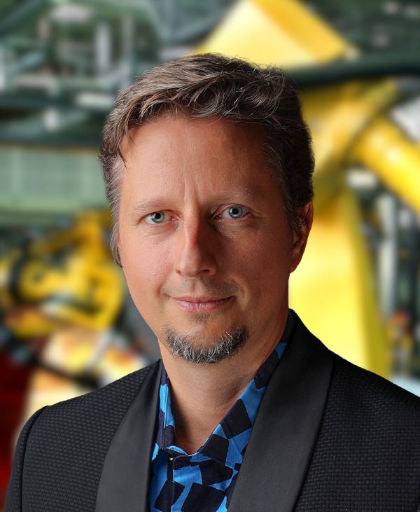

Dr. Ronald Müller boasts over two decades of expertise in the global Imaging market. His passion for the diverse applications of this technology began well before he earned his doctorate in Computer Vision and Machine Learning. Since 2014, Dr. Müller has been driving the growth of ambitious companies in the Imaging industry, worldwide. As Managing Partner of Vision Markets he established the leading management consulting firm with four synergistic service areas: Strategy, M&A, Marketing, and Recruitment.
In addition to his consultancy work, Dr. Müller is an active contributor to the global vision community. He is a sought-after speaker at industry conferences, a regular author in trade publications, and serves on the Board of Directors of the EMVA, the Advisory Board of the Image Sensors conference, and several innovation award juries.


Kazuko Nishimura received her B.E. degree from Osaka University, Japan, in 1995 and received her PhD degree from Kobe University, Japan, in 2022. She has since been engaged in the research and development of high-speed ADCs, optical transceivers and image sensors. Currently she is the Senior Researcher of the R&D Center, Sony Semiconductor Solutions Corporation, Japan. Her technical focus is in the advanced CMOS image sensor circuit and system development.

Dan McGrath has over 45 years of experience in pixel device physics—CCD, CIS, and ToF—and in integrating image-sensor process enhancements into manufacturing. His career covers the full spectrum of image-sensor design: small consumer pixels; large, high-sensitivity pixels; sensors for infrared through visible to gamma rays; and particle detection. His recent work focuses on photon counting for night vision, scientific, and time-of-flight applications, and he has maintained a long-standing interest in dark current. Dan is Senior Technology Fellow for Image Sensors at TechInsights, working in reverse engineering, and is also a visiting researcher at ISAE Supaero in Toulouse, studying dark current in quantum image sensors. He earned his Ph.D. in physics from Johns Hopkins University. Dan has advanced image-sensor technology through roles at Texas Instruments, Polaroid, Imaging Devices, Atmel, Eastman Kodak, Aptina, BAE Systems, and GOODiX, collaborating with fabs in the USA, France, Italy, and Taiwan. His publications include the first megapixel CCD, the foundations of dark current spectroscopy, and recent work on dark current in quantum image sensors.
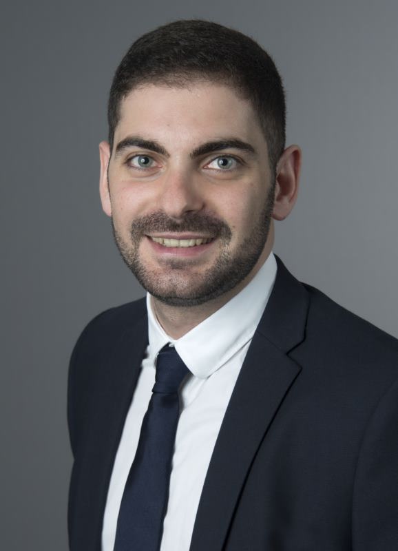

Anas Chalak is Technology & Market analyst at Yole Group. He is a member of the Imaging team. Anas contributes on a day-to-day basis to follow imaging technology activity to provide market and technology analysis, as well as contributing to the production of relevant reports and projects. Previously, Anas carried out research focusing on integrated mid-infrared photonics. Later, he worked as a research engineer on the optical optimization of a 3D FMCW lidar system in CEA-Leti, France. Anas obtained a Master’s in Nanoscale Engineering from École Centrale de Lyon, France.

Albert Theuwissen received the degree in electrical engineering and his PhD from the Catholic University of Leuven (Belgium) in 1977 and 1983 respectively. In 1983 he joined Philips Research Labs (the Netherlands) and in 2002 he started working for DALSA. His whole career he was involved in R&D of solid-state image sensors.
He issued several patents and he is author or coauthor of 240+ technical papers, including a textbook "Solid State Imaging with Charge Coupled Devices". He acted as general chairman of the International Image Sensor Workshop in ’97, ’03, ‘09 and in ’15, and as International Technical Program Chair of the ISSCC2010.
In 2001, he became part-time professor at the Delft University of Technology, the Netherlands. He left DALSA in 2007, and founded Harvest Imaging. Since then he is fully focusing on training, teaching and consulting in the field of solid-state imaging technology.
In 2011 he received the Electronic Imaging of the Year Award and in 2017 he was elected as the President of the International Image Sensor Society.
_2.png?ext=.png)
Sara Pellegrini is a pixel architect leading the advanced photonics sensors technology development activities in STMicroelectronics’ centre of competence for imaging in Edinburgh. In this role she works in close collaboration with the silicon, process, module and system R&D teams to define and develop the Imaging Division photonics pixel roadmap and specification. In addition to this she works with external collaborators on several R&D projects within STMicroelectronics’ Imaging PhD Programme.
Sara graduated in Electronics Engineering at the Politecnico di Milano in 1999 and received her PhD in Physics from Heriot-Watt University in 2006. She has authored and presented several papers on SPAD and SPAD-based systems and applications.

Andras Pattantyus-Abraham has been working on commercializing quantum-dot based image sensors since 2013, when he joined Invisage Technologies to work on RGB and NIR imaging. He joined Apple in 2017, where he became Senior Manager of QD R&D. In 2020, he transitioned to STMicroelectronics and became Director of Advanced Materials R&D for QD sensors, now focused on SWIR sensing and imaging. In October 2024, he founded BestQD Solutions LLC to help accelerate the adoption of low-cost QD-based SWIR imagers. He has deep expertise in QD synthesis, quality control and QD-based optoelectronics design, processing, testing and application development.
He has B.Sc.’s in Engineering Physics and Mathematics from Queen’s University and a Ph.D. in Chemistry from the University of British Columbia. He also worked as a postdoc and principal scientist under Ted Sargent at the University of Toronto, where he did pioneering work on depleted heterojunction QD photovoltaics.

Jeroen Hoet is the CEO and co-founder of eyeo, a Dutch startup specializing in image sensors enabled with advanced nanophotonic color-splitting. eyeo aims to redefine image sensing by overcoming traditional filter limitations and enhancing image quality, resolution and low-light performance.

Algorithms expert with 15 years experience in AI/Deep Learning, Computer Vision, Computational Photography and Image Processing. From 2013-2018, Tom developed core technology at Apple powering the iPhone’s Portrait Mode. During his early career as a PhD / Post-Doc researcher, he developed inverse imaging technology and published papers in areas such as De-blurring, Super-Resolution, and Depth Estimation, with applications to novel computational camera architectures including Light Fields and coded imaging. He later lead teams in industry and drove innovation at two startups, applying cutting edge Machine Learning methods to Computer Vision problems, applied to automated Photo Retouching products and large scale image recognition, retrieval and representation learning systems.
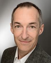

As a dedicated "Principal" ZEISS expert, Markus Cappellaro follows the trends in image sensors technology from the customer and user perspective for a wide range of applications in light microscopy. It stretches from documentation in routine applications to scientific imaging at the highest level. This is his basis for his many years as product manager for digital camera systems at Carl Zeiss Microscopy, where he is responsible for a complete digital camera portfolio. He holds a degree in Electrical Engineering and Information Technology from the Technical University of Munich and loves sports fencing as one of his favorite pastimes because, like his job, it requires precision, speed and strategy.
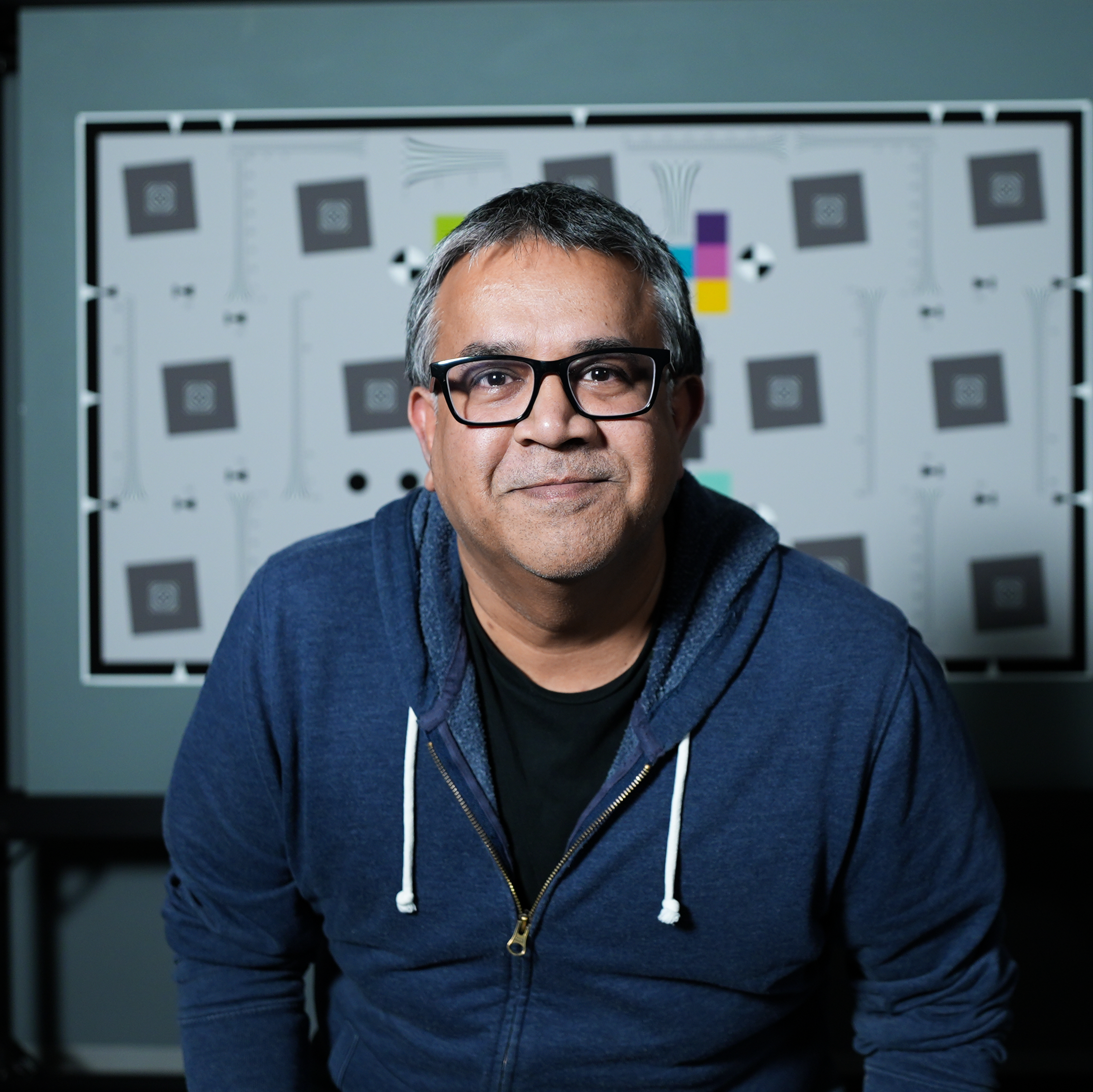

Harish holds multiple degrees in the fields of physics, computer science and engineering. Beginning at Texas Instruments, he advanced to Director of Design in the High Volume Linear Org where his team led sensor designs in the field of Touch Sensing for consumer electronics. Transitioning to Apple in 2014, he contributed significantly to the development of inertial sensors before switching gears and joining the Camera Team. Over the next 6 years, he specialized in the field of 2D and 3D Cameras as a key contributor to features like Face ID and the Lidar Scanner for iPhones.
Currently, Harish serves as Principal Engineer in Cameras & Depth Systems @ Meta Inc. focusing on identifying and integrating sensing technologies for AR and VR applications.
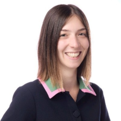

Leveraging a strong background in machine vision, she drives sensor specification and system level use case definition, including architectures that combine on chip image processing with SoC computation to optimize power, bandwidth, and overall system cost. Her work spans ecosystem enablement with development tools, reference designs, and strategic partnerships. She holds an engineering degree in semiconductor physics and two master’s degrees – in optics and semiconductors, and in business administration.
Prior to joining STMicroelectronics, she worked at Teledyne on imaging solutions for advanced machine vision systems.

Roberto Buttaci brings over 20 years of experience in the semiconductor industry, with the past decade focused on the industrial image sensor sector. As head of the industrial image sensor sales and marketing team in Europe, Roberto draws on both technical expertise and a practical understanding of market dynamics and customer needs. Known for his collaborative approach and thoughtful leadership, he is committed to supporting innovation and sustainable growth within the industry.
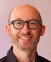

Arno holds an engineering degree in Media Technology from TU Ilmenau (Germany) and has gained more than 18 years of experience in the automotive sector. He has previously held various roles at Tier1s in the area of hardware development and decided to move into the semiconductor industry in 2021, joining Valens Semiconductor as FAE for Europe. Arno supports customers in successfully integrating the next-generation of sensor connectivity into automotive ADAS systems and machine-machine applications.


Alastair Attard is Director of Business Development at UTAC Group. He has a Bachelor’s degree in Mechanical Engineering and an Executive MBA, and brings over 19 years of experience in the semiconductor assembly & test. Alastair has previously held positions at STMicroelectronics in MEMS and SiP process engineering and package development, and at Besi where he managed the process development group for advanced die attach technologies. Alastair joined UTAC in 2018 and today is responsible for business development of semiconductor assembly and test solutions with particular focus on MEMS, Sensing, and Advanced Packaging.
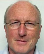

Robert Henderson is a Professor of Electronic Imaging in the School of Engineering at the University of Edinburgh. He obtained his PhD in 1990 from the University of Glasgow. From 1991, he was a research engineer at the Swiss Centre for Microelectronics, Neuchatel, Switzerland. In 1996, he was appointed senior VLSI engineer at VLSI Vision Ltd, Edinburgh, UK where he worked on the world’s first single chip video camera. From 2000, as principal VLSI engineer in STMicroelectronics Imaging Division he developed image sensors for mobile phone applications. He joined University of Edinburgh in 2005, designing the first SPAD image sensors in nanometer CMOS technologies in the MegaFrame and SPADnet EU projects. This research activity led to the first volume SPAD time-of-flight products in 2013 in the form of STMicroelectronics Flightsense series which perform an autofocus assist function in more than 150 different smartphone models, recently passing the 1 billion module milestone. He benefits from a long term research partnership with STMIcroelectronics in which he explores medical, scientific and high speed imaging applications of SPAD technology. In 2014, he was awarded a prestigious ERC advanced fellowship. He is a Fellow of the Royal Society of Edinburgh.
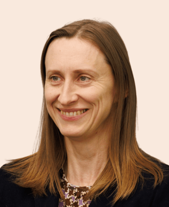

Silvie Luisa Brázdilová, PhD, is a Software Engineer at onsemi, focused on innovative initiatives and optimization projects. She has an academic background in Mathematics and Computer Science and previous experience in the aerospace industry. Her current work involves applying artificial intelligence to the design of nanophotonic image sensors, supported by enhanced simulation techniques.

.png?ext=.png)
Uwe Artmann studied Photo Technology at the University of Applied Sciences in Cologne following an apprenticeship as a photographer and finished with the German ’Diploma Engineer’. He is the CTO at Image Engineering, an independent test lab for imaging devices and manufacturer of all kinds of test and calibration equipment for these devices. He is also the head of the standards department within VCX-Forum e.V. and member of various international workgroups regarding standardization of image quality measurement including IEEE and EMVA.
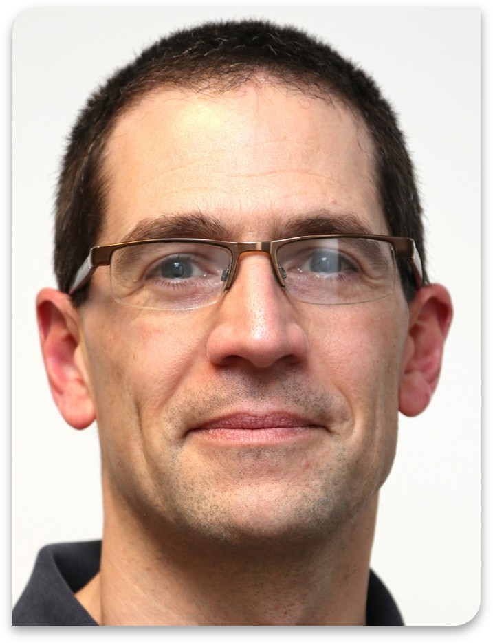

Darryl graduated from the University of Surrey, UK, in 1995 with a degree in electrical and electronic engineering.
He initially worked as an ASIC designer on telecommunications chips before moving into an imaging position in 2006 where he set up his first image quality labs focusing on mobile, medical but predominantly automotive image sensors. Since then he has worked on a wide range of both raw sensors and ones which include ISPs for both human viewing and ADAS applications.
Darryl has also been an active member of the IEEE P2020 working group since early 2018 and led the flare metric which can be found in the now released IEEE 2020-2024 standard.
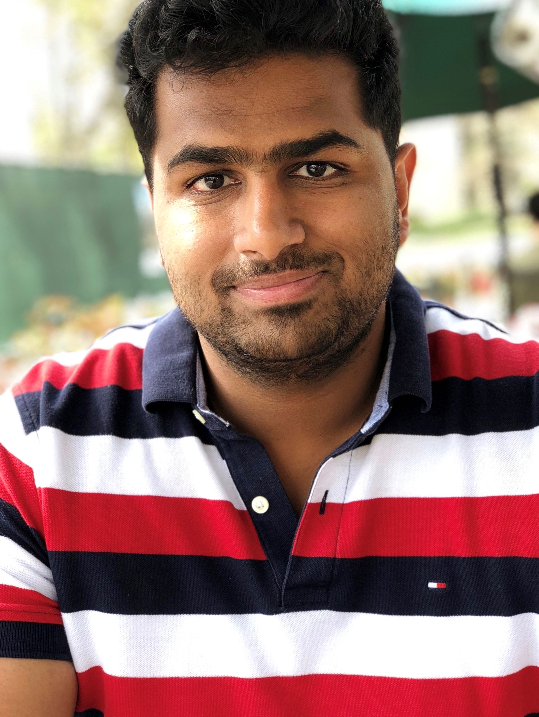
Abhinav Agarwal is currently a Member of Technical Staff with Forza Silicon (Ametek Inc.) and was instrumental in recently establishing a Forza India design center in Bangalore. He is a technical lead for various CMOS image sensors chips designed at Forza Silicon in applications ranging from cinematography, automotive and biomedical. As a lead author, he has presented papers at several prominent conferences like the International Image Sensor Workshop (IISW), IEEE VLSI Symposium on Circuits and Technology. He received the best student paper award at the IEEE Custom Integrated Circuits Conference in 2020. Abhinav is also passionate about improving the design and verification flows related to CMOS Image Sensors and has presented multiple collaborative articles with Siemens EDA at the Design Automation Conference (DAC). Prior to his role Forza, Abhinav was graduate researcher at Caltech working in implantable medical devices resulting in several US patents.

.png?ext=.png)
Dr. Augusto José Carimatto is an experienced integrated circuit (IC) designer and currently serves as Head of the IC Department at Pi Imaging Technology. He holds a degree in Electronics Engineering from the National Technological University (UTN), Buenos Aires, an M.Sc. from the University of Troyes, France, and a Ph.D. from Delft University of Technology (TU Delft), The Netherlands, specializing in Single-Photon Avalanche Diode (SPAD) sensors and ASIC design. With over fifteen years of experience in microelectronics, Dr. Carimatto has developed extensive expertise in the design of advanced integrated circuits for demanding scientific and industrial applications. Throughout his career, he has been actively engaged in research spanning a broad range of domains, including Positron Emission Tomography (PET), LiDAR, Artificial Intelligence, Neural Networks, Genetic Algorithms, Robotics, and Support Vector Machines. During the final years of his doctoral research, Dr. Carimatto focused on SPAD image sensors, developing multiple integrated sensor architectures for LiDAR, PET, and high-speed imaging applications. His work encompassed the design of neural networks, high-performance bus architectures, high-bandwidth memory systems, specialized microprocessors for image sensors, and custom back-end compilers, demonstrating a comprehensive command of both hardware and algorithmic design.


Jörg Kunze is the Group Leader of the Research Team at the Basler AG in Ahrensburg, Germany. Since joining Basler in 1998, he has invented over 50 patents and applications. He currently also serves as Basler’s patent manager.
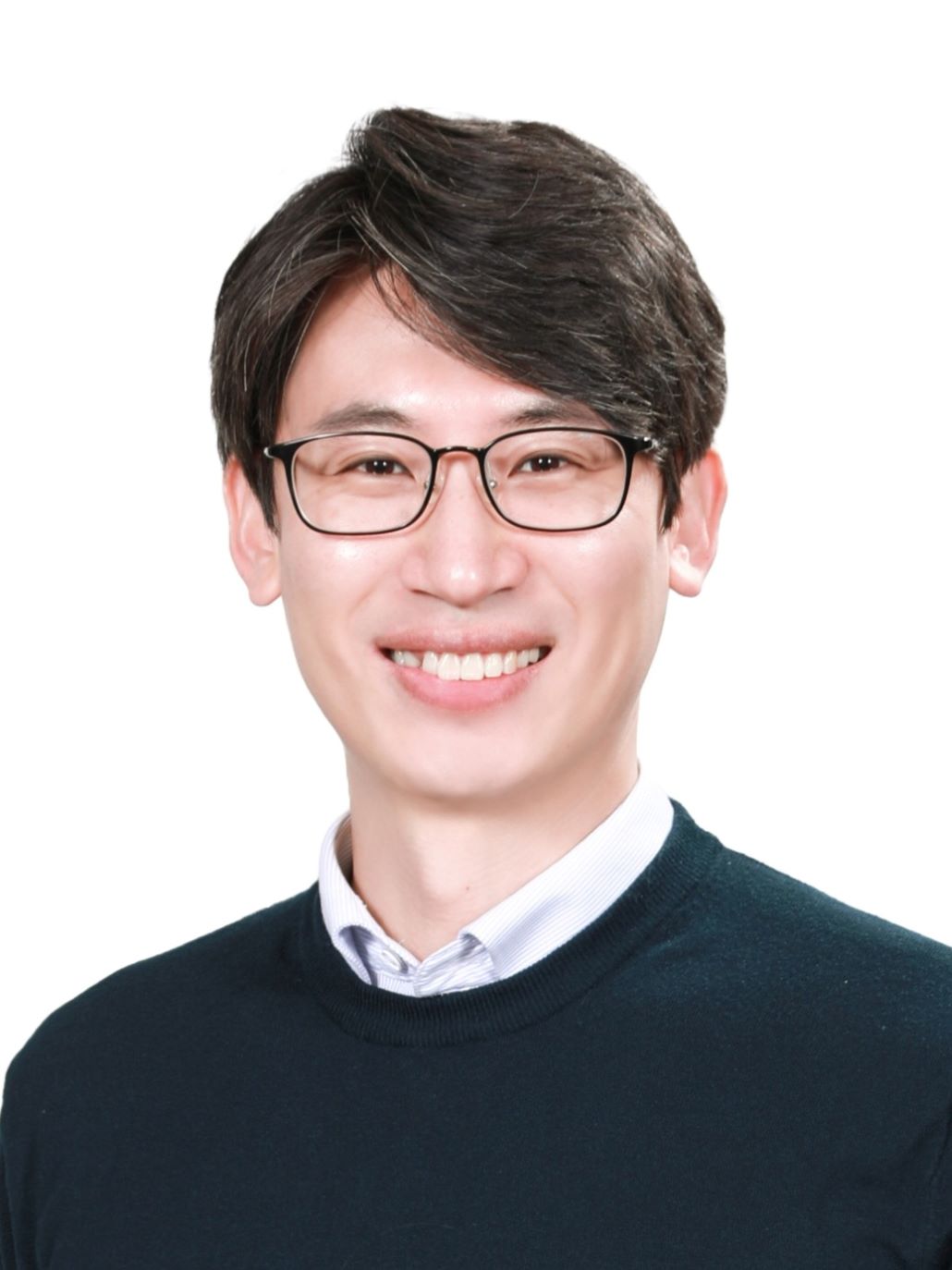

Min-Woong Seo received his Ph.D. degree from Shizuoka University, Hamamatsu, Japan, in 2012, with a dissertation focused on low-noise, high-dynamic-range CMOS image sensors using high-performance analog-to-digital converters (ADCs). From 2012 to 2014, he was a JSPS Research Fellow at the Imaging Devices Laboratory of Shizuoka University. He then served as an Assistant Professor at the Research Institute of Electronics (RIE), Shizuoka University, from 2014 to 2016, and as an Associate Professor from 2016 to 2018. In 2018, he joined the Semiconductor R&D Center (SRDC) at Samsung Electronics, Hwaseong, Korea.
His research interests include CMOS imaging devices, low-noise imaging, time-resolved image sensors, global-shutter image sensors, pixel-/column-parallel ADCs for imagers, and mixed analog/digital circuit design. He has been serving on the Technical Program Committee (TPC) of Electronic Imaging (EI) since 2018 and of the International Solid-State Circuits Conference (ISSCC) since 2024. He has also been a steering committee member of the Korean Image Sensor Society (KISS) since 2024, a board member of the International Image Sensor Society (IISS) since 2025, and an advisory board member of Image Sensors (IS) Asia since 2025.

Dirk has been developing and specifying space detectors for more than three decades, since joining MBB in Ottobrunn in 1988 until his retirement from Airbus Defence and Space in Ottobrunn in December 2023.
Throughout his career, he has maintained his fascination with developing sophisticated optical instruments for specific applications.
He is keen to apply his deep understanding of highly specialised detector technologies, coupled with his ability to engage with stakeholders to solve their challenges.
Dirk has been a member of SPIE since March 1995. He received a Dipl. Ing. degree in Photo(graphic) Engineering from the University of Applied Sciences in Cologne in 1988, after studying electrical engineering (1978 - 1983) at the Technical University of Munich, Department of Electrical Engineering.
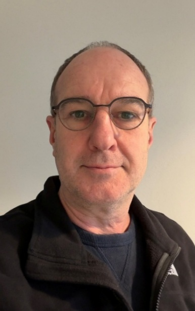
Jeroen Rotte graduated in 1995 with a BSc in Electrical Engineering from HZ University of Applied Sciences in Vlissingen, the Netherlands. He began his career at Philips, later Grass Valley, where he contributed to the transition from CCD to CMOS image sensors for broadcast applications and worked on multiple generations of CMOS image sensors operating in UHD with high frame rate (HFR) and high dynamic range (HDR) capability. His work covered sensor architecture, imager correction algorithms, debugging, characterization, and HDR video processing.
After serving as Group Leader Image Sensors at Grass Valley, Jeroen joined Gpixel in 2023 as Sr. Imaging Specialist, where he applies his expertise in sensor architecture and imaging systems to a new generation of CMOS image sensor designs across diverse application areas.

Ed Goffin is Vice President of Product Marketing with Pleora Technologies and is responsible for product and marketing strategies to ensure the company delivers the best solutions to its customers. Over his 25-year career, he has held corporate communications, marketing, and investor relations roles in the telecom and machine vision industries. Ed is an elected member of the Association for Advancing Automation (A3) Vision & Imaging Technology Strategy Board providing strategic direction and industry leadership for the association's 1300+ members in the robotics, AI, and automation industries.